Antennas are an integral part of any wireless system. They are used to efficiently transform guided
electric signals into freely propagating electromagnetic waves. Many different types of antennas
exist, ranging from simple structures consisting of a single straight wire to complex phase
controlled antenna arrays with many hundreds of carefully spaced radiating elements. A number of
important characteristics are used to describe an antenna. Among these are:
When defining the different antenna parameters, usually only the far-field from the antenna is
considered. This is done due to the fact that the far-field from any antenna is a TEM wave
propagating in the r direction of the spherical coordinate system, where the
antenna is located in origin, see figure below.
The spherical coordinate system with the antenna at origin.
The far-field is defined as the electromagnetic field in the region for which the distance r
is larger than the far-field distance Rff , given by*
Rff = 2D2 / λ0
for D ≥ 2.5 λ0
Rff = 5D for 0.4
λ0 ≤ D ≥ 2.5 λ0
Rff = 2λ0 for
D≤ 0.4 λ0
Where D is the maximum physical dimension of the antenna, and λ0 is
the wavelength corresponding to the operating frequency. A theoretical antenna, which radiates
its energy uniformly in all directions in space is called an isotropic antenna. In practice it is
impossible to construct such an antenna, but the concept is useful for defining other antenna
parameters, such as the antenna directivity and gain.
Directivity of the antenna describes how the antenna radiates power in different directions.
The directivity D(θ, φ) is the ratio of the radiation
intensity U in the direction (θ, φ), to the radiation
intensity averaged over all directions.
The term "directivity" is often used with no particular direction specified. When this is the case,
the direction of maximum directivity is assumed. The directivity of an antenna is often expressed in
decibels with respect to the directivity of a reference antenna. An isotropic antenna with
D = 1 is often employed as the reference antenna and the term dBi is used.
The antenna bandwidth describes the range of frequencies over which the antenna is able to
efficiently radiate or receive energy. The antenna bandwidth is typically specified in terms of VSWR
or |S11| over a frequency range. The antenna is typically assumed to operate efficiently
when VSWR < 2 or |S11| < −10 dB.
* Peter Meincke and Jens Vidkjær. Introduction to Wireless RF System Design. 2011
Antenna Array
For some applications it is impossible to meet the gain or radiation pattern requirements with one
antenna. By combining multiple antennas into a one- or two-dimensional antenna array an
improved antenna performance can be achieved. An antenna array can be used too achieve:
An increase in the gain.
An increase in the bandwidth.
Cancellation of interference from specific directions.
Active control of the radiation pattern (by using a technique called
phased array).
A simple way to understand the theory behind antenna arrays is by considering the following example:
n isotropic antennas, spaced by λ0/2 are positioned along the
z-axis direction, as illustrated in figure below.
The geometry of the example array.
A plane wave is arriving at an angle θ to the z-axis. The
E-field of the wave as a function of position can be expressed as:
Where r is the position of a receiving antenna element and
is the wave vector, which describes the spatial phase variation of a plane wave*.
The signal at the terminals of each of the antenna elements can thus be expressed as:
For the entire array, the received signal will be the sum of the signal from each of the antennas:
A plot of the magnitude of Y(θ) versus the angle and the number of antennas
n is shown in figure below
Magnitude of an antenna array output vs. θ and
n.
From the figure it can be seen that although the individual antennas are isotropic, when placed in an
array, their combined radiation pattern will gain directivity. The directivity will depend on the
number of elements in the array – the more elements, the more directive the antenna.
The total radiation pattern, Fa , of a non-steered array (in a phase
controlled array a complex weight is applied to the individual elements) is typically expressed
through the array function, which takes the positions of the individual antennas into
account:
Where Fi(θ,φ) is the radiation pattern of a single antenna element, or
the individual antenna element, if different antenna types are used in the same array.
* Peter Joseph Bevelacqua. Antenna arrays (phased arrays).
Antenna Impedance
The antenna impedance relates the voltage and the current at the antenna input terminals
Vt = ItZA. The antenna impedance is generally a
complex, frequency dependent quantity, which can be expressed as ZA =
RA + jXA, where RA is the antenna
resistance and XA is the antenna reactance.
Attenuators
Attenuators are electronic devices, which are used to reduce the power of a given signal without
distorting the signal waveform. Attenuators are typically passive and are made of resistor divider
networks. The two commonly used attenuator networks are called the π-pad and the
T-pad attenuators. The circuit diagrams for the two network types are shown in the
following figures.
π-padattenuator
T-padattenuator
As it can be seen from the figure, both attenuator types are symmetrical. This is done in order to
equate the impedance on the ports, thereby making them interchangeable. The input and output
impedances of the ports are typically designed to match the characteristic impedance of the
system where the attenuator is going to be used, Zin = Zout = Z0.
The design equations for a π-pad attenuator are:
,
.
And for a T-pad attenuator:
.
Where K = 10LdB/20 is the ratio of current, voltage
or power, corresponding to a desired attenuation LdB.
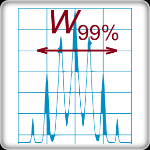
Beamwidth
In addition to the radiation pattern, antennas are also characterized by their beamwidths and
sometimes sidelobe levels.
The main lobe (beam) of the antenna is the region around the direction of maximum
radiation, while the antenna sidelobes are smaller beams, radiating in other directions.
The half power beamwidth, or sometimes just the beamwidth, of an antenna, is
typically defined as
the angular separation over which the radiation pattern decreases by 3 dB from the peak of the main
beam. These parameters
are illustrated in the example radiation pattern below.
An example radiation pattern with indications of the main lobe, the sidelobes and the
beamwidth
Complex Signal Representation
Often, when dealing with sinusoidal signals, it is cumbersome to operate with the real valued signal
notations. In order to simplify the mathematical operations, a representation of the real
signals using complex phasors is often used. The advantages of using complex signal notation in
mathematical analysis are:
The derivations are simplified, as trigonometric equations are turned into algebra of exponents.
Addition of signals is performed by simple vector addition in the complex plane.
A phasor is a complex number that is a function of time. Let us consider the complex number
ejφ, where φ =
2πf0t = ω0t. This number,
also called a complex exponential, is depicted as the tip of the red vector in the complex
plane in the figure below.
ejφ in the complex plane.
As time t increases,φ, the phase angle of the complex exponential increases, while the
amplitude of the signal is kept constant. The spiral path created by the phasor motion is shown in
the following figure, where time is added as the third dimension.
The continuous motion of the phasor’s tip as a function of time and the real and
imaginary parts of ejφ.
The real and imaginary parts of ejφ are shown as projections onto the
real/time and the imaginary/time planes respectively, demonstrating Euler’s identity:
ejφ = cos (φ) +
j sin (φ)
If a second phasor, e-jφ, which is rotating in the opposite direction of
ejφ is introduced into the first figure (shown in blue), the sum of the
two complex exponentials, due to the nature of complex conjugation, will always result in a real
valued number:
ejφ + e-jφ =
cos (φ) + j sin (φ) + cos (φ) −
j sin (φ)
ejφ +
e-jφ = 2 cos (φ)
cos (φ) = 1/2
(ejφ + e-jφ)
A similar expression can be derived for a sine:
sin (φ) = j/2 (e-jφ -
ejφ).
Using these equations, a real signal can be written in complex form
Coplanar Waveguide, Grounded
Coplanar Waveguide with Lower Ground Plane, aka CPWG, is a popular type of planar
transmission line, and is a part of the coplanar waveguide transmission line family.
The geometry of a CPWG transmission line.
CPWG, similarly to the microstrip transmission line, consists of a conductive trace of width
W, deposited on a grounded dielectric substrate of thickness d. The difference
lies in the conductive trace being flanked by ground planes from both sides, with g being
the gap distance.
The CPWG lines have a number of advantages over microstrip lines:
They simplify shunt and series mounting of surface mounted devices.
They reduce radiation loss, as the top-side ground planes shunt the electric field and keep
it close to the board surface.
They reduce spacing design considerations for other components and traces.
Their characteristic impedance is less sensitive to the presence of a metallic shield cover
in close proximity to the board surface.
Similar to microstrip transmission lines, the design equations for the CPWG lines are based on
approximations to the static or quasi-static solutions.
Directional Couplers
Directional couplers are passive devices, whose purpose is to couple a certain part of the energy
flowing in a transmission line to another port. Directional couplers are often symmetrical 4-port
devices. A block diagram symbol for a directional coupler is shown in the following figure.
A block diagram symbol for a directional coupler.
As it can be seen from the figure, the 4 ports are called the input port, the
transmited port, the coupled port and the isolated port. An important
property that defines a directional coupler is that it only couples energy flowing in the direction
(from the input port to the transmitted port) to the coupled port. The energy flowing into the
transmitted port is coupled to the isolated port, which is often terminated in a matched
load. A directional coupler is characterized by the following parameters:
Coupling factor - is the primary property of a directional coupler, which
describes the amount of energy being coupled from port 1 to port 3. The coupling factor is a
negative quantity, defined by:
.
Operational Bandwidth - is the frequency range over which the coupler maintains its
operational parameters as well as a good impedance match on all of the ports.
Coupling loss - is the power in the port 1 to port 2 transmission, lost due to coupling
to port 3. It is defined as:
.
Insertion loss - is the power lost in the transmission from port 1 to port 2. It is
defined by:
.
In an ideal directional coupler the insertion loss will entirely consist of the coupling loss.
Isolation - is defined by the power leakage from on output port to another output port,
when the other ports are terminated into matched loads:
.
The coupler parameters can also be expressed in terms of a scattering matrix, which for an ideal
directional coupler will look like**:
.
Where κ and τ are complex frequency dependent quantities. Insertion loss and coupling
factor can be expressed by:
.
One of the widely used methods of constructing directional couplers is by using coupled transmission
lines, as shown in the following figure:
Layout of the directional coupler based on coupled lines.
The parameters of the coupler are determined by the geometry – the width of the transmission lines,
the length of the parallel sections, and the separation distance between them. For TEM transmission
lines, such as the stripline and the coaxial lines these parameters can be determined through
techniques such as the even-odd mode analysis and conformal mapping. For quasi-TEM
lines, such as microstrip lines, the results can be obtained by numerical simulations or
quasi-static techniques*.
* David M. Pozar. Microwave Engineering. John Wiley & Sons, Inc., fourth edition, 2012.
Antenna Gain
Antenna gain is a term derived from the directivity, which takes the antenna radiation efficiency
into account:
G(θ,φ) =
D(θ,φ)ηrad
Similar to directivity, when no particular direction is specified, the direction of maximum gain is
assumed. Gain is also often expressed in decibel with respect to the gain of a reference antenna,
for which a lossless isotropic antenna is often employed.
Gain is sometimes expressed through another parameter, denoted the antenna effective area or the
antenna apertureAe,
G = 4πAe/λ2
which is a measure of how effective an antenna is at receiving. Ae is
related to physical area of the antenna through
Ae= Aρe , where
ρe is the antenna aperture efficiency.
Microstrip Transmission Lines
One of the most widely used planar transmission line types is a microstrip transmission
line. This type of transmission line is particularly popular due to simple fabrication
process, as it can be integrated on a printed circuit board (PCB). The geometry of a microstrip line
is depicted in the figure below:
The geometry of a microstrip transmission line.
As it can be seen from the figure, the microstrip line consists of a thin conductor of width
W on a grounded dielectric substrate of thickness d. The relative
permittivity of the dielectric substrate is εr. The analysis of the
microstrip line is complicated by the fact that a small part of the fields propagate through the air
above the conductor, while the rest propagates through the dielectric, as shown in the figure below:
Electric and magnetic field lines around a microstrip line.
Due to the difference in the dielectric properties of the two media, the microstrip transmission line
can not support a pure TEM wave, as the phase velocity of the wave will be different in the air
(vp = c) and inside the dielectric
(vp = c / √
εr).
In practical applications the dielectric thickness is chosen to be electrically thin: d
<< λ. By doing this, the fields can be considered to be quasi-TEM, and good
approximations for the transmission line parameters can be obtained by curvefitting the static or
quasi-static solutions*. The phase velocity and the propagation constant can be expressed
as:
Where k0 is the wave number of a plane wave in free space
k0 = ω√
μ0ε0, and
εe is the effective dielectric constant, which satisfies 1 <
εe < εr and can be interpreted as
the dielectric constant of a homogeneous dielectric medium that equivalently replaces air and
dielectric regions of the microstrip line. εe is dependent on
such factors as the substrate thickness, conductor width and the frequency. An approximation for the
effective dielectric constant for a microstrip line is given by:
The width of the microstrip line for a given characteristic impedance and substrate
εr can be calculated from the W/d ratio found by
applying the following design equation:
Where terms A and B are:
* David M. Pozar. Microwave Engineering. John Wiley & Sons, Inc., fourth edition, 2012.
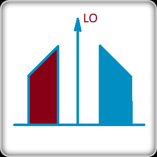
1 dB compression point (P1dB), and 3rd-order intercept point (IP3)
Linear two-ports, such as linear amplifiers for example, often have a fixed gain over the specified
bandwidth. If the output power is plotted versus the input power, as shown in figure below, the
relationship will be linear and the slope of the line will be equal to the gain. In real amplifiers,
as the magnitude of the input signal grows larger, at some point the amplifier will start to
saturate and the gain will start to decrease. When this happens, the amplifier is said to be
operating in the compression region.
Illustration of the 1 dB compression point, which corresponds to the input power
that causes the gain to decrease 1 dB.
The linearity of an amplifier is typically described by its 1 dB compression point (P1dB),
which is the input power level that causes the gain to decrease 1 dB from the expected linear output
(in some component datasheets P1dB is specified as the output level, at which a 1 dB drop occurs).
When designing circuits that contain amplifiers, it is important to keep the input signal level
below P1dB, as the amplifier will start producing harmonics of the input signal on its output, when
it enters the non-linear region. The second and above order harmonics, which are produced by an
amplifier operating in the non-linear region, typically lie outside of the amplifier bandwidth and
cause no problems. However, non-linearity also produces a mixing effect if two or more signals are
present at the input. If the two signals are close together in frequency, some of the generated
frequencies, called the intermodulation products, can occur within the amplifier bandwidth
and will thus interfere with the main signals, causing intermodulation distortion (IMD).
The problem is illustrated in the figure below.
Illustration of intermodulation products present in an amplifier output signal due
to non-linearity.
The third-order intercept point describes the capability of an amplifier to suppress the
2f1 − f2 and 2f2 −
f1 two-tone, 3rd-order intermodulation distortion. In this approach
the 3rd-order intercept point (IP3) is defined as the theoretical location, where the two
3rd-order products and the theoretical output signal become equal in power, as the input power is
increased. This point is illustrated in the first figure.
Patch Antennas
One of the most popular types of planar antennas, are patch antennas, sometimes referred to as
microstrip antennas. Patch antennas are particularly attractive due to their simplicity, low cost
and ease of fabrication, as they, similarly to microstrip transmission lines, can be manufactured
during the standard PCB manufacturing process.
A simple rectangular patch antenna with a microstrip feedline.
A simple rectangular patch antenna, fed by a microstrip transmission line, is shown in figure above.
As it can be seen from the figure, the antenna consists of an electrically thin
(h « λ0) conductive patch placed on a dielectric
substrate with relative permittivity εr, above a ground plane. The
operating frequency of the antenna is determined by the length of the patch, l, which is
chosen to be close to λ0 / 2. The approximate center frequency is then
given by:
f0 ≈ c / (2l
√
εr)
The principle of operation of a rectangular patch antenna can be understood by considering the
antenna as an open circuited transmission line. As the current at the end of the transmission line
is zero, due to the open end, it takes its maximum value at the center of the patch. The voltage, on
the other hand, is 90° out of phase, so it takes its maximum value at the open end of the
transmission line, its minimum value at the center, and its maximum negative value at the feed
point, as illustrated in figure below.
The voltage and current distributions over the length of a rectangular patch
antenna.
The E-field lines underneath the patch antenna are also sketched in this figure. The fringing fields
near the surface of the patch antenna appear to have a horizontal component in the same direction at
both edges, adding up in phase, and thus giving rise to the radiation*. The fringing
fields are also responsible for a down shift in the actual resonance frequency of the patch,
compared to the one calculated using formula above. This shift occurs due to an apparent extension
of the patch length by the fringing fields, which can be modelled as radiating slots. This apparent
extension can be approximated by**:
The input impedance of a theoretical patch antenna is infinitely high, due to the 0 current at the
feed point. In practice, the input impedance of a patch antenna with
l = W is
Zin ≈ 400 Ω. As such high impedance is impractical, a
number of ways exist to lower it. Some of the most popular ways are:
By increasing the width W of the patch.
By using an inset feed, to shift the feed point to a more favourable impedance.
By using a coaxial feed from the bottom of the board at correct offset from the patch edge.
The two latter methods are illustrated below.
Patch antenna with inset feed.
Patch antenna with coaxial feed.
Rectangular patch antennas are linearly polarized, with the direction of polarization going along the
length of the patch. These antennas are generally very narrowband, with a bandwidth as low as 3% of
the center frequency. The bandwidth can be slightly improved by increasing the width of the patch. A
number of methods have been proposed to make significant improvements of the patch bandwidth.
* Peter Joseph Bevelacqua. Microstrip (Patch) Antennas.
** Aruna Rani and R. K. Dawre. Design and Analysis of Rectangular and U Slotted Patch for Satellite
Communication. International Journal of Computer Applications, 12(7), December 2010.
Polarization
The polarization of an antenna describes the orientation of the electric field of the radio wave
emitted by the antenna in relation to the surface of the Earth.
The polarization is dependent on the type of the antenna, its construction and its spatial
orientation. Generally, the polarization should be considered as a sum over
time of projections of the electric field onto a plane perpendicular to the motion of the radio
wave. In most cases, the polarization varies over time, which gives
the projected shape an elliptical form. Special cases of polarization are circular polarization
(where both axes of the ellipse are equal) and linear polarization (where
the projection falls onto one of the axes).
Practical antennas are never polarized in a single mode. Hence, a parameter called cross
polarization is used to describe the ratio of the opposite polarization component
to the desired polarization component.
Radiation Efficiency of the Antenna
The power accepted by the antenna depends on the antenna resistance,RA, and the
current at the antenna input terminals,It ,:
Pt = 1/2
RA |It|2 .
For a lossless antenna, all of the accepted power is converted into
unguided electromagnetic waves and radiated. If the antenna is lossy, a part of the accepted power
is dissipated by the antenna and converted into heat, while the remaining part is radiated. The
antenna radiation efficiency, ηrad, is defined as the ratio of the radiated
power to the accepted power:
ηrad = Prad /
Pt .
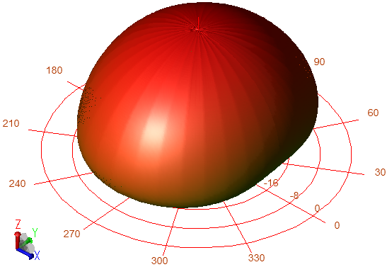
Radiation Pattern of the Antenna
A graph, that shows the relative field strength versus the direction at a fixed distance
from the antenna in the far-field is called the radiation pattern of the antenna.
The radiation pattern is a plot of a three-dimensional function
F(θ,φ),
which varies with both θ and φ in a spherical coordinate
system. An example of
a radiation pattern is shown in the following figure.
An example radiation pattern of a patch antenna
Sometimes, in order to avoid complex three-dimensional plots, the plot is given as the magnitude of
the normalized field
strength versus θ for a constant φ (called the E-plane
pattern) and the magnitude of the
normalized field strength vs. φ for θ = π/2 (called the
H-plane pattern)*.
* David K. Cheng. Field and Wave Electromagnetics. Addison-Wesley Publishing Company, Inc, second
edition, 1989.
Scattering Parameters
When dealing with high frequency components such as transmission lines, filters, amplifiers,
attenuators and couplers, a component can typically be represented as an n-port network.
A 2-port network with incident and reflected waves at both ports
As it is difficult to measure the individual voltages and currents at high frequencies (microwave
range and above), but easier to measure the ratios of the incident and the reflected waves, a
scattering matrix approach is often more convenient for the description of n-port networks.
A 2-port network, such as the one depicted above, can thus be characterized by using a
scattering matrix:
Where the generally complex matrix elements, the scattering parameters or the
S-parameters, represent the relations between the incident and the reflected waves of the
network ports as follows:
V1− =
S11V1+ +
S12V2+
V2− =
S21V1+ +
S22V2+
S11 and S22 are the reflection coefficients on port 1 and 2,
respectively, when the opposite port is terminated in a matched load. S21
represents the transmission from port 1 to port 2, when port 2 is terminated in a matched load and
vice versa for S12.
Knowledge of the reflection coefficients can be used to calculate the input impedances of the network
ports:
This App was created at the Technical University of Denmark. The provided information is based on the
Notes developed by Prof. Jens Vidkjær.
Project Coordinator and Developer:
Vitaliy Zhurbenko
Contributors:
Mads Doest
Daniel Areñas Mayoral
Denis Tcherniak
Emilie Jong
Disclaimer:
All information provided in this App is provided for information purposes only, and we make no
guarantees of any kind.
Any links to external web resources are provided as a courtesy and should not be considered as an
endorsement.